Half a millennium ago, Dutch spectacle-makers put lenses together in new ways and invented the telescope and the microscope. Novel instruments have been the key to scientific discovery throughout history.
In particle physics, new technologies brought the field into the electronic era, enabling the discovery of the top quark and the Higgs boson, and contributing to establishing the Standard Model of fundamental particles and forces.
“Technologies are transformative,” says physicist Marcel Demarteau, a senior scientist at Argonne National Laboratory. “New technologies have made it possible to measure the universe at the dawn of time, probe the dark sector, study the asymmetry between matter and anti-matter, and track down the secrets of the elusive neutrino.”
Whether the search is for supersymmetric particles or distant quasars, detectors are the sine qua non of particle physics and cosmology. Particle physics has pushed detector technology forward for decades, and new materials and innovative industrial techniques offer the potential to do so again. New technologies can find their way into daily life as well.
Thick chips for searching the skies
Twenty years ago, scientists assumed the pull of gravity was slowing the universe’s expansion. The international Supernova Cosmology Project, based at Lawrence Berkeley National Laboratory, set out to measure how the universe was changing by observing Type Ia supernovae, exploding stars whose consistent brightness makes them dependable standard candles for establishing cosmic distances.
By comparing Type Ia distances and redshifts—a direct measure of expansion, which stretches the light traveling from the supernovae to longer wavelengths—the SCP team and the rival High-Z Supernova Search Team discovered, to their astonishment, that the universe is actually expanding at an accelerating rate.
This was the first evidence that dark energy is pushing the universe apart, but finding it wasn’t easy: The most advanced detectors of the day performed poorly with highly redshifted light.
Saul Perlmutter, who heads the SCP, recalls that in 1994, “we were having problems with the red sensitivity and internal reflections at red wavelengths in existing astronomical CCDs.”
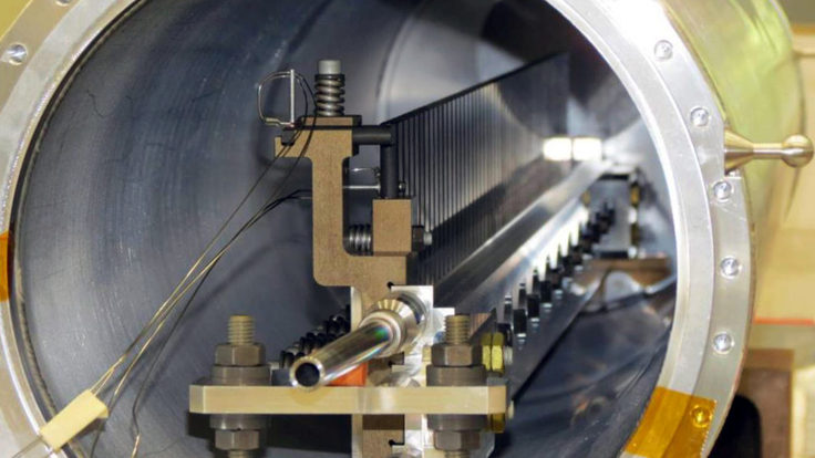
At the time, CCDs—the charge-coupled devices found in digital cameras—were the cutting-edge technology for replacing photographic plates in astronomy. CCDs capture photons and convert them to electrical signals. But typical astronomical CCDs have to be shaved to a tissue-thin 20 millionths of a meter to allow charge carriers to reach the circuitry on the other side of the chip.
While that works great for blue light, it’s bad news for red and infrared light, which are long-wavelength and can sail right through a thin chip; what doesn’t get through bounces back and forth, causing interference fringes. Not only did thin astronomical CCDs have problems with red light, they were expensive. So many were damaged during thinning that the survivors were worth more than 50,000 dollars each.
Existing CCDs were a weak point for the SCP and high-redshift astrophysics generally. Over lunch in the Berkeley Lab cafeteria in 1994, Perlmutter explained the difficulties to physicist David Nygren, a man Demarteau calls “the best instrumentalist in the field.”
Nygren suggested that Perlmutter talk with an electronics engineer named Steve Holland. Holland had just developed an advanced silicon-based detector for another project, the ill-fated Superconducting Super Collider, which was planned but never constructed. Like most silicon detectors for accelerators, it was a rugged chip about the thickness of a postcard.
Off and running, Holland and his colleagues morphed the particle-catcher into a light catcher. A thin window on the light-collecting side doubled as an electrode, creating voltage that guided blue-light charges straight through to the chip’s electronics, while the chip’s thickness caught long-wavelength photons and eliminated fringe-producing reflections.
Manufacturing processes took time to perfect, so the supernova teams had to discover dark energy without the advanced CCD. Nevertheless its impact on cosmology has been remarkable. The Berkeley Lab design is a key part of several leading modern experiments that probe the nature of dark energy: the third Sloan Digital Sky Survey’s Baryon Oscillation Spectroscopic Survey; the Hyper Suprime-Cam on the 8.2-meter Subaru Telescope; and the innovative Dark Energy Camera that powers the Dark Energy Survey.
“The red sensitivity of the CCDs was one of the critical new features that made DECam worth doing,” says Brenna Flaugher, head of Fermilab’s Astrophysics Department, who led the development of Dark Energy Camera.
The advanced CCD also contributed to significant progress in medical imaging. Its photodiode component not only captures long-wavelength red light but other radiation as well. Early on, the technology was licensed for cameras that diagnose heart disease by the Digirad Corporation, one of the top players in the world’s $2 billion nuclear imaging market.
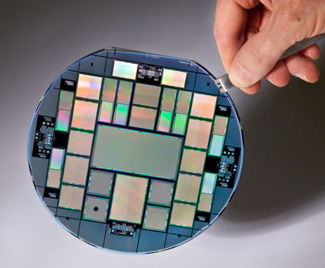
The Berkeley Lab CCD is known for its high sensitivity to light, particularly long-wavelength red light.
A multiple-purpose layer cake
Perlmutter and Holland’s story is one of many. Over and over in particle physics, researchers see a need for new kinds of instrumentation and find unique solutions that go on to revolutionize the field—and, often, other fields as well.
In 2007, Ray Yarema, then head of the Electrical Engineering Department in Fermilab’s Particle Physics Division, saw a coming wave of collider experiments that would pose critical technical problems. As particle accelerators produced collision events more efficiently, experimentalists would require wide arrays of trackers to deal with tsunamis of data.
The biggest challenges would arise closest to where the beams collided. A new generation of detectors was needed to combine pixel arrays, which determine where particles strike, with readout electronics. They had to have higher resolution, quicker processing and better radiation hardness than anything then in the works.
Yarema argued that a solution was already at hand in the form of three-dimensional integrated circuits, or 3D ICs, developed by industry. These could “do all kinds of neat calculations [and] deliver nearly instantaneous processing with far less power,” says Demarteau, who was then working at Fermilab. The task was to integrate pixel sensors, which register where particles strike, into a new kind of 3D IC.
Fermilab organized an international consortium of a dozen physics laboratories to produce a demonstration 3D pixel-readout chip. They chose Tezzaron Semiconductor, a leader in the 3D field, as an industrial partner.
“We were designing 3D chips as early as 2004, and we’d already gotten to the show-stoppers and fixed them,” says Gretchen Patti, a Tezzaron technical staff member and the company’s spokesperson. Although their specialty was memory chips, Patti says the prospect of working with a national laboratory was exciting. “The great thing about Fermilab is that they are pushing the boundaries of what 3D can do. Sensors are a wonderful application for 3D.”
Together, the laboratory consortium overcame design and manufacturing challenges to develop a highly successful 3D chip. Each problem that’s overcome opens the way for new applications of 3D integrated circuitry for science and the consumer.
Grzegorz Deptuch, who has led Fermilab’s Pixel Design Group since Yarema’s retirement, says that for many instruments, the ability to make a 3D chip with any combination of sensors, processors and memory, using both analog and digital elements, “is the right answer.”
As for computing power, “one can imagine storing a terabyte of information on something the size of a postage stamp,” says Demarteau. “Think about putting that in your next smart phone.” This potential power and flexibility account for a 3D IC market estimated at $3 billion, climbing toward $7.5 billion by 2019.
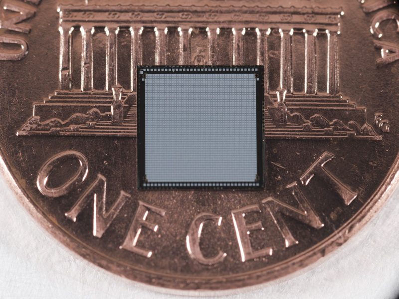
A Tezzaron-Fermilab 3D chip.
Shaping the light
Today, instrumentation development is more important than ever. When even small experiments can cost millions, “time and cost mean the projects have to succeed, so there’s little risk-taking,” Demarteau says. Yet, at the same time, “there has to be investment in instrumentation with a healthy portfolio of risk.”
Early in 2012, Waruna Fernando, then a postdoc at Argonne’s Center for Nanoscale Materials, called Demarteau’s attention to an article in the journal Nano Letters: A group at the University of California, Berkeley, described using graphene—single sheets of carbon atoms—to manipulate light.
Demarteau recalls, “Waruna’s first thought was that we could make a new kind of optical modulator,” a device that can shape the frequency, amplitude, and other properties of the light signal, including how many channels a single fiber can carry. “It was an intriguing idea, and we wondered what else we could do with it—perhaps use it for developing a new kind of particle detector.”
The worth of any detector increasingly depends on fast, smart transmission of its data. “The limitation on signal transfer in an optical fiber is how many bits per second you can push through it,” says Demarteau. “Essentially you have to turn the light on and off really fast.”
His team is developing two kinds of modulator. Their initial effort—which he calls a “crude concept”—lays bare the fiber’s cladding to expose the glass core, then wraps it with two sheets of graphene. The double layer interacts with the evanescent electromagnetic field generated by lightwaves moving through the core; electrodes attached to the graphene tune the voltage. Demarteau explains, “Graphene kills the light, but applying a voltage to the graphene makes it transparent.”
Crude, maybe, but this kind of modulator is expected to couple efficiently to the optical signal, consuming little power at minimal cost. Demarteau’s group has already demonstrated proof of the principle.
A more sophisticated design would create ring waveguides—structures that steer light—each tailored to resonate at a specific wavelength. The resonant wavelength travels around the ring, “leaking” to adjacent silicon waveguides, which read out the signal. The technique could filter out unwanted frequencies in astronomical observations, for example. Whether made of graphene or other materials, ring waveguides could be tuned to different frequencies, enabling a single fiber to carry hundreds of channels.
“This is really pie in the sky,” Demarteau says, “but theoretically we could make a modulator that operates at 400 or 500 gigabits per second per channel, for high-speed data transmission totalling trillions of bits per second. With that kind of capacity, your detector could stream any amount of data.”
Applications in the “real world” would be tremendous, he adds, “from streaming many millions of phone calls over a single fiber, to providing near instantaneous access to massive amounts of data anywhere in the world.”

Graphene, which has a hexagonal structure, is a promising material for high-speed data transmission.
Into the future
The implications of any new technology, like any scientific result, are sometimes more exciting than what can be imagined in advance—and almost always different. After inventing the radio in 1887 to prove the existence of electromagnetic waves, Heinrich Hertz explained its other applications with the dismissive phrase, “it's of no use whatsoever.” Ten years later, J.J. Thompson used a cathode ray tube to determine that electrons were discrete particles, a discovery that was not of much interest to people outside of physics—until the advent of telephones, radios, TVs, computers, smart phones... with no end in sight.
Today, scientists are more alert to the possibilities. From proven successes to pie-in-the-sky, the foremost goal of instrument designers is to extend the reach of science. But they also know that what’s transformative for science can be transformative for society. So they keep a sharp eye open for the gadgets that could trigger tomorrow’s telecommunications, electronics or medical diagnostics.
“Innovation and improvement in the quality of life go hand in hand,” Demarteau says. “Investment in R&D for new technologies in particle physics, combined with advances in other areas of science, will not only open the wonders of the cosmos to us all but improve the quality of our lives, as it has in the past.”