Particle accelerators earned an important place on the semiconductor assembly line decades ago, and today their role in silicon wafer manufacturing processes continues to grow in complexity and scope.
As a silicon wafer makes its way down the assembly line, it may pass through dozens of particle beams produced by accelerators in a process known as ion implantation. Born out of the national labs, this process embeds fast-moving particles in the wafer at specific locations, depths and concentrations, permanently changing the semiconductor's electrical qualities by selectively creating an abundance of electrons or electron vacancies at specific locations.
These electron-rich or electron-depleted areas, in combination with other transistor components affixed to the regions, work like rivers of charge to guide electrons around a semiconductor in precisely controlled ways.
Advances in ion implantation have helped manufacturers to pack more transitors into an integrated circuit, revolutionizing computing speed and power and reducing room-sized machines to pocket-sized devices.
"Ion implantation is an absolutely necessary technology in the way we build devices, and its use has been growing," says Larry Larson, an engineering professor at Texas State University at San Marcos who previously worked for National Semiconductor, a Silicon Valley-based chip manufacturing firm acquired by Texas Instruments in 2011. "Every time a factory is built, they need some number of ion-implantation machines in the factory, and the number of machines per factory has grown over the years."
Today there are an estimated 12,000 ion-implantation accelerators operating worldwide and an average of 300 new ones are purchased each year, with the lion's share purchased by the semiconductor industry.
To meet manufacturing demands, the implanting processes become incrementally more exacting and elaborate each year, with researchers fine-tuning the number of particle beams a single wafer encounters and the angle at which each beam hits the wafer. The speed of the implantation process is also ramping up to meet manufacturing demand; today, the quickest implanters can process about 300 wafers an hour.
Alexander Wu Chao, a professor at SLAC National Accelerator Laboratory and editor of the journal Reviews of Accelerator Science and Technology, says that ion-implantation accelerators are essential to today’s—and tomorrow’s—advanced electronics.
"They are becoming much more sophisticated and much more precise as required by modern semiconductors," he says. While ion implantation is often used to treat flat semiconductor surfaces, there are also applications that require implantation on the sides of raised, gridded surfaces, which pose far more challenges in achieving uniform doping.
Accelerator advances in the semiconductor industry have contributed to the exponential growth of computing technology, Chao continues, saying that he expects "a continuing evolution of accelerator technology to meet the increasing demands in the years to come."
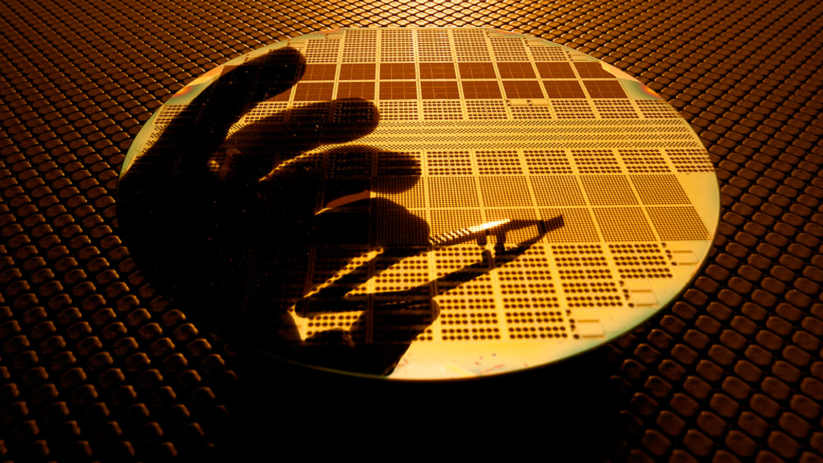
Above: A single silicon wafer, like the one seen here, is typically bombarded with ions of several different elements. Boron, arsenic and phosphorous are among the elements most commonly used in the semiconductor industry.