The Gordon and Betty Moore Foundation has awarded $13.5 million to Stanford University for an international effort, including key contributions from the Department of Energy’s SLAC National Accelerator Laboratory, to build a working particle accelerator the size of a shoebox. It’s based on an innovative technology known as “accelerator on a chip.”
This novel technique, which uses laser light to propel electrons through a series of artfully crafted glass chips, has the potential to revolutionize science, medicine and other fields by dramatically shrinking the size and cost of particle accelerators.
“Can we do for particle accelerators what the microchip industry did for computers?” says SLAC physicist Joel England, an investigator with the 5-year project. “Making them much smaller and cheaper would democratize accelerators, potentially making them available to millions of people. We can’t even imagine the creative applications they would find for this technology.”
Robert L. Byer, a Stanford professor of applied physics and co-principal investigator for the project who has been working on the idea for 40 years, says, “Based on our proposed revolutionary design, this prototype could set the stage for a new generation of ‘tabletop’ accelerators, with unanticipated discoveries in biology and materials science and potential applications in security scanning, medical therapy and X-ray imaging.”
The chip that launched an international quest
The international effort to make a working prototype of the little accelerator was inspired by experiments led by scientists at SLAC and Stanford and, independently, at Friedrich-Alexander University Erlangen-Nuremberg (FAU) in Germany. Both teams demonstrated the potential for accelerating particles with lasers in papers published on the same day in 2013.
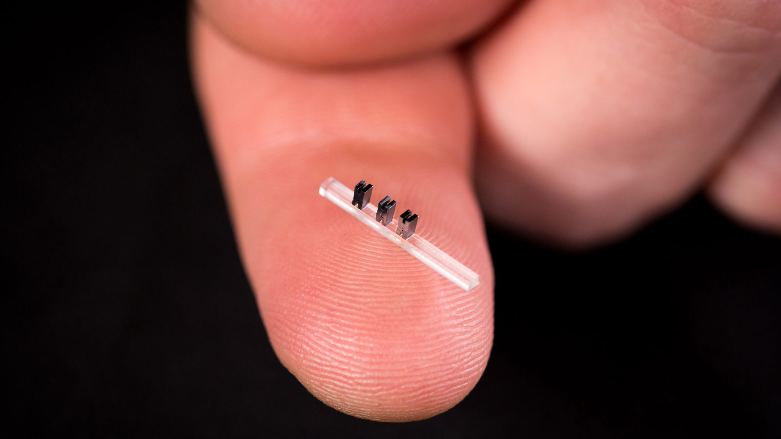
In the SLAC/Stanford experiments, published in Nature 1 Demonstration of electron acceleration in a laser-driven dielectric microstructure, electrons were first accelerated to nearly light speed in a SLAC accelerator test facility. At this point they were going about as fast as they could go, and any additional acceleration would boost their energy, not their speed.
The speeding electrons then entered a chip made of silica and traveled through a microscopic tunnel that had tiny ridges carved into its walls. Laser light shining on the chip interacted with those ridges and produced an electrical field that boosted the energy of the passing electrons.
In the experiments, the chip achieved an acceleration gradient, or energy boost over a given distance, roughly 10 times higher than the existing 2-mile-long SLAC linear accelerator can provide. At full potential, this means the SLAC accelerator could be replaced with a series of accelerator chips 100 meters long, roughly the length of a football field.
In a parallel approach, experiments led by Peter Hommelhoff of FAU and published in Physical Review Letters 2 Laser-based acceleration of nonrelativistic electrons at a dielectric structure demonstrated that a laser could also be used to accelerate lower-energy electrons that had not first been boosted to nearly light speed. Both results taken together open the door to a compact particle accelerator.
A tough, high-payoff challenge
For the past 75 years, particle accelerators have been an essential tool for physics, chemistry, biology and medicine, leading to multiple Nobel prize-winning discoveries. They are used to collide particles at high energies for studies of fundamental physics, and also to generate intense X-ray beams for a wide range of experiments in materials, biology, chemistry and other fields. This new technology could lead to progress in these fields by reducing the cost and size of high-energy accelerators.
The challenges of building the prototype accelerator are substantial. Demonstrating that a single chip works was an important step; now scientists must work out the optimal chip design and the best way to generate and steer electrons, distribute laser power among multiple chips and make electron beams that are 1000 times smaller in diameter to go through the microscopic chip tunnels, among a host of other technical details.
“The chip is the most crucial ingredient, but a working accelerator is way more than just this component,” says Hommelhoff, a professor of physics and co-principal investigator of the project. “We know what the main challenges will be, and we don’t know how to solve them yet. But as scientists we thrive on this type of challenge. It requires a very diverse set of expertise, and we have brought a great crowd of people together to tackle it.”
The Stanford-led collaboration includes world-renowned experts in accelerator physics, laser physics, nanophotonics and nanofabrication. SLAC and two other national laboratories, Deutsches Elektronen-Synchrotron (DESY) in Germany and Paul Scherrer Institute in Switzerland, will contribute expertise and make their facilities available for experiments. In addition to FAU, five other universities are involved in the effort: University of California, Los Angeles, Purdue University, University of Hamburg, the Swiss Federal Institute of Technology in Lausanne (EPFL) and Technical University of Darmstadt.
“The accelerator-on-a-chip project has terrific scientists pursuing a great idea. We’ll know they’ve succeeded when they advance from the proof of concept to a working prototype,” says Robert Kirshner, chief program officer of science at the Gordon and Betty Moore Foundation. “This research is risky, but the Moore Foundation is not afraid of risk when a novel approach holds the potential for a big advance in science. Making things small to produce immense returns is what Gordon Moore did for microelectronics.”