Particle detectors are the eyes of physicists, peering closely into particle events to help us understand the basic laws of nature.
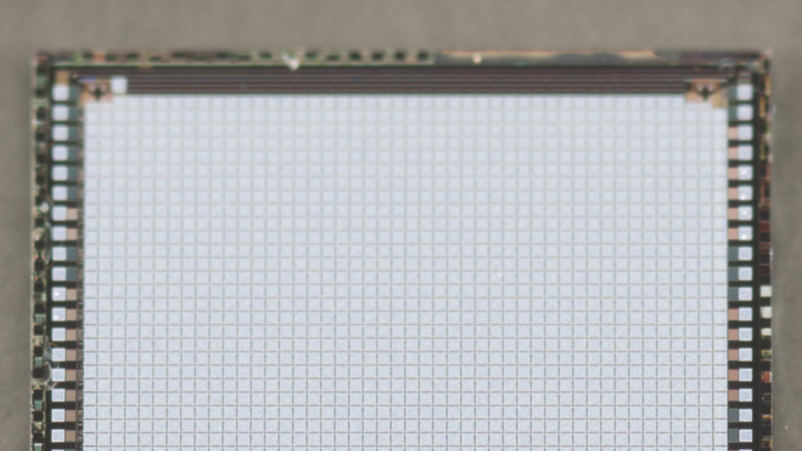
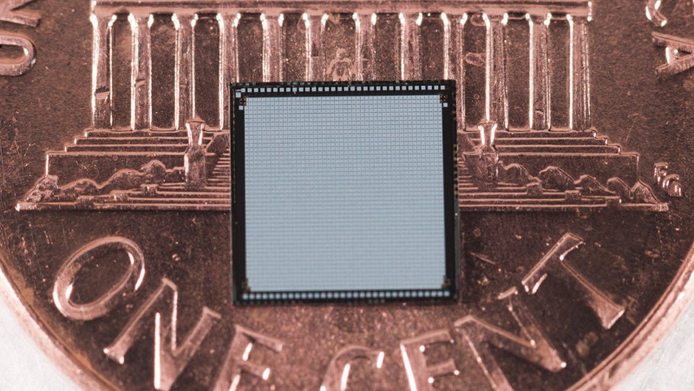
To develop the kind of sight needed to view the complex particle events of future experiments, researchers are transforming detection technology by developing new, intelligent detectors. They are pushing past the limits of two-dimensional chips, the current technology, by adding to them another dimension. The three-dimensional integrated chip, or 3DIC, will be key for future detectors.
"3DIC technology should be looked at as a toolbox that can allow us to make a transformational change in the way pixel detectors are and will be designed in the future," says Gregory Deptuch, who heads a group that's working on 3DIC R&D at Fermilab.
The "3D" term refers to the chip's layered arrangement of circuitry, as contrasted with a single-plane, side-by-side arrangement. The design allows for shorter connections between the chip's elements, which in turn allows for increased functional density, buying more space and making for more efficient pathways along which to shepherd information.
"Some people think we just take a chip, cut it in half and stack it," says physicist Ted Liu. "But what we're doing is architecturally changing things at the design level to take full advantage of the 3DIC technology to dramatically improve the performance."
Industry currently develops 3D chips for cameras and computers. Recognizing 3DIC's potential for high-energy physics, in 2005 now-retired Fermilab engineer Ray Yarema initiated the 3D-chip R&D program at Fermilab. This stimulated great interest among detector community worldwide, and in 2008 HEP researchers formed an international consortium, led by Fermilab, to facilitate 3DIC developments for various uses in science. Now the laboratory is working with several industrial partners, primarily with Tezzaron Inc. located near Fermilab, to fabricate prototype chips.
With the 3DIC's increased functional density, the chips can be intelligent enough to discriminate between signal and background almost as soon as a collision's signals come out of the gate, helping to filter what is important and dispense with what is not.
"If you are able to discriminate the signals, you are the winner," Deptuch says.
Fermilab researchers have been testing 3DIC prototypes for various detector components to be used in CMS, ATLAS, the ILC and even in photon science projects. The tests confirmed what researchers had expected—3D is the way to go.
"Both science and industry are looking at 3DIC as a cheaper alternative to building smaller and denser chips than the traditional 2D design," says engineer Jim Hoff.
One of the laboratory's main efforts is to develop a processor for tracking particles as they spring from the interaction point, performing fast pattern recognition and feeding information to a trigger system, which is a filter for particle physics events. The technology is expected to appear in CMS following its high-luminosity upgrade.
"This new circuitry could effectively integrate the entire original CDF silicon tracking trigger system—four racks of electronics—into one 3D chip," Liu says.
"The international community recognizes 3D technology as crucial for advancing particle physics instrumentation," Deptuch says. "It's not an exaggeration to say we're the world leader in 3DIC research in HEP."
This article appeared in Fermilab Today on Thursday, Oct. 11.